
티스토리 뷰
IDEC 강의 영상을 보고 정리한 내용입니다.
https://www.idec.or.kr/vod/apply/view/?pay=&search_val=CPU&no=273
반도체설계교육센터
강의제목 CPU 설계 및 응용 구분 부산대 / 설계강좌 / 초급/중급 / 이론+실습 강의시간 13시간 열람기간 16일 이용료(일반) 무료 이용료(학생) 무료 강의개요 SoC 설계를 위해서 CPU를 설계하고 응용할
www.idec.or.kr
저번까지 설계한 CPU의 구조이다.
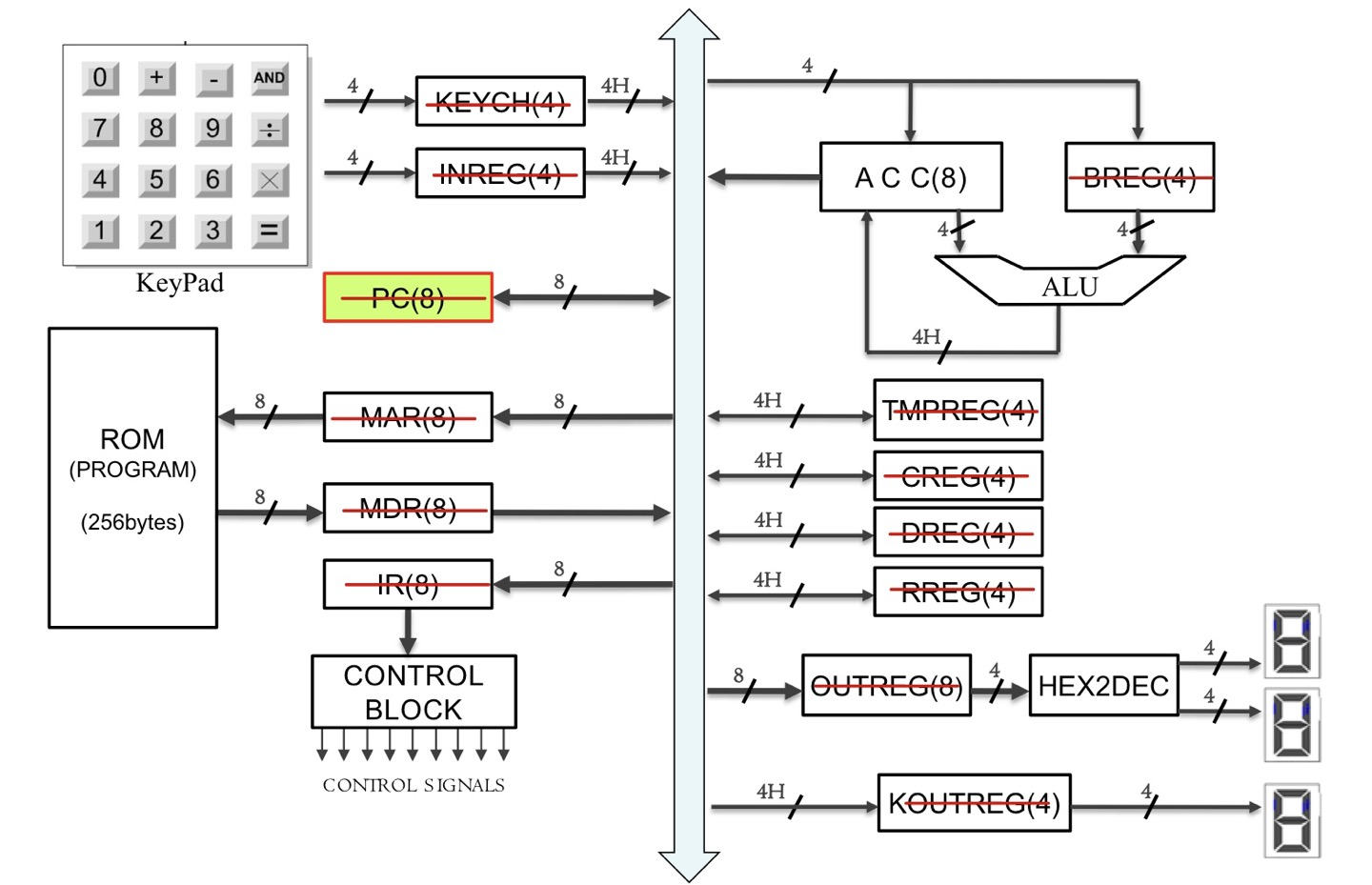
이번에는 ACC(Accumulator, 누산기)를 설계할 것이다.
ACC(Accumulator)
ACC와 ALU를 함께 나타낸 구조는 다음과 같다.
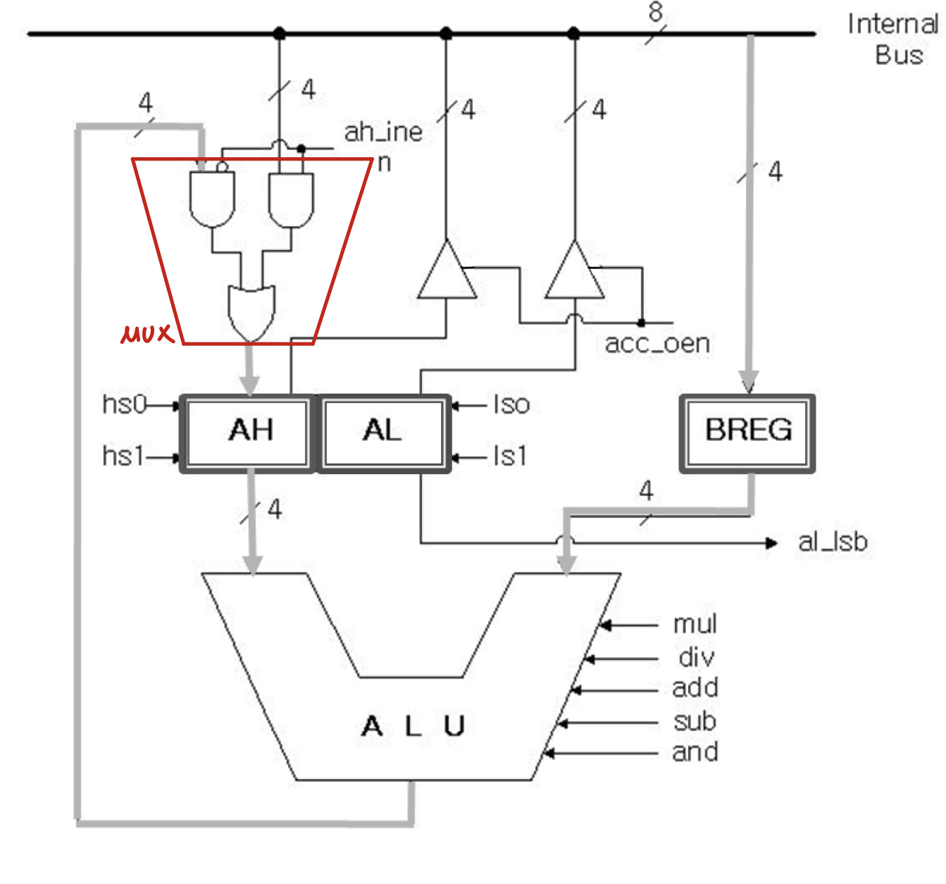
AH + AL이 누산기이고 양옆의 신호가 제어신호이다.
ALU의 출력과 입력 모두 누산기를 거치며 Internal bus의 data line은 AH에 연결되어있다.
제어신호를 정리하면 다음과 같다.
| AH | AL | ||||
| hs1 | hs0 | operation | ls1 | ls0 | operation |
| 0 | 0 | No change | 0 | 0 | No change |
| 0 | 1 | Shift Right | 0 | 1 | Shift Right |
| 1 | 0 | Shift Left | 1 | 0 | Shift Left |
| 1 | 1 | Data Load (from bus) |
1 | 1 | Parallel Shift (AL = AH) |
ACC 안의 제어신호는 4to1MUX로 구현했고 universal shift register 구조를 가지고있다.

위의 그림을 이해하면 AL의 제어신호(ls)가 (1,1)일 때 AH값을 어떻게 AL로 가져올 수 있는지 알 수 있다.
위의 그림을 AH shift register라고 한다면 (A4,A3,A2,A1)이 AL shift register의 (I4,I3,I2,I1)으로 연결되면 된다. 자세한 회로는 뒤에 첨부했다.
4to1 MUX
위의 구조를 만들기위해 4to1 MUX를 만들어야한다. case구문을 사용하였다. case문을 사용할 때는 모든 case에 대하여 값이 있어야한다. 그렇지 않으면 의도하지않은 latch가 생겨 성능이 급격하게 떨어진다.
module mux4to1(n,s,dout);
input [3:0] n;
input [1:0] s;
output dout;
reg a;

always@(s,n)begin
case(s)
2'b00 : a=n[0];
2'b01 : a=n[1];
2'b10 : a=n[2];
2'b11 : a=n[3];
endcase
end
assign dout = a;
endmodule
Universal shift register

module shreg(carry_msb,carry_lsb,c,clr,clk,data_in,data_out);
input carry_msb, carry_lsb, clr, clk;
input [1:0] c;
input [3:0] data_in;
output [3:0] data_out;

wire [3:0] a;
//mux4to1(n,s,dout);
mux4to1 mux0({data_in[3], data_out[2], carry_msb, data_out[3]},c,a[3]);
mux4to1 mux1({data_in[2], data_out[1], data_out[3], data_out[2]},c,a[2]);
mux4to1 mux2({data_in[1], data_out[0], data_out[2], data_out[1]},c,a[1]);
mux4to1 mux3({data_in[0], carry_lsb, data_out[1], data_out[0]},c,a[0]);

reg4 reg4(a,1'b1,1'b1,clk,clr,data_out);

endmodule
`timescale 1ns / 1ps
module tb_shreg;
//Inputs
reg carry_msb;
reg [1:0] c;
reg [3:0] data_in;
reg clr;
reg clk;
reg carry_lsb;
//output
wire [3:0] data_out;
//UUT
shreg UUT(
.carry_msb(carry_msb),
.c(c),
.data_in(data_in),
.clr(clr),
.clk(clk),
.carry_lsb(carry_lsb),
.data_out(data_out)
);
// Initialize inputs
always #50 clk = ~clk;
initial begin
carry_msb = 0;
c=2'b00;
data_in = 4'b1100;
clr = 1;
clk = 0;
carry_lsb=0;
#100;clr=0;
#100;c=2'b11;
#100;c=2'b00;
#100;c=2'b01;
#200;c=2'b00;
#100;c=2'b10;
#200;c=2'b00;
#100;end
endmodule
제어신호에 맞게 동작하는 것을 확인할 수 있다.
ACC
Shift register 2개로 ACC를 설계할 수 있다. AH의 output을 AL의 input으로 연결해주면 된다.

module acc(ah_reset, clr, clk, ah_in, ah_inen, aludata, carry_out, hs, ls, ah_out, al_out);
input ah_reset, clr, clk, ah_inen, carry_out;
input [1:0] hs;
input [1:0] ls;
input [3:0] aludata;
input [3:0] ah_in;
output [3:0] ah_out;
output [3:0] al_out;
wire [3:0] a;
//MUX
assign a=(ah_inen)?ah_in : aludata;
// shreg(carry_msb,carry_lsb,c,clr,clk,data_in,data_out);
shreg shreg_ah(.carry_msb(carry_out), .carry_lsb(al_out[3]), .c(hs), .clr((clr|ah_reset)), .clk(clk), .data_in(a), .data_out(ah_out));
shreg shreg_al(ah_out[0], carry_out, ls, clr, clk, ah_out, al_out);
endmodule
`timescale 1ns / 1ps
module tb_acc;
reg ah_reset;
reg clr;
reg clk;
reg [3:0] ah_in;
reg[3:0] aludata;
reg ah_inen, carry_out;
reg [1:0] hs, ls;
wire [3:0] ah_out;
wire [3:0] al_out;
acc UUT(.ah_reset(ah_reset),
.clr(clr), .clk(clk), .ah_in(ah_in),
.aludata(aludata), .ah_inen(ah_inen),
.carry_out(carry_out),.ah_out(ah_out),
.al_out(al_out),.hs(hs), .ls(ls)
);
always #50 clk = ~clk;
initial begin
aludata = 4'b0010;
ah_in = 4'b0101;
ah_reset = 0;
clk = 0;
ah_inen = 0;
carry_out = 0;
hs=2'b00;
ls=2'b00;
clr = 1;
#100; clr=0;
#100; hs=2'b11;
#100; hs=2'b00;
#100; ah_inen=1; hs=2'b11;
#100; hs=2'b00; ls=2'b11;
#100; ls=2'b00;
#100; hs=2'b01; ls=2'b01;
#100; hs=2'b00; ls=2'b00;
#100; hs=2'b10; ls=2'b01;
#100; hs=2'b00; ls=2'b00;
#100; hs=2'b10; ls=2'b10;
#100; hs=2'b00; ls=2'b00;
#100; ah_reset=1;
#100; ah_reset=0;
#100;
end
endmodule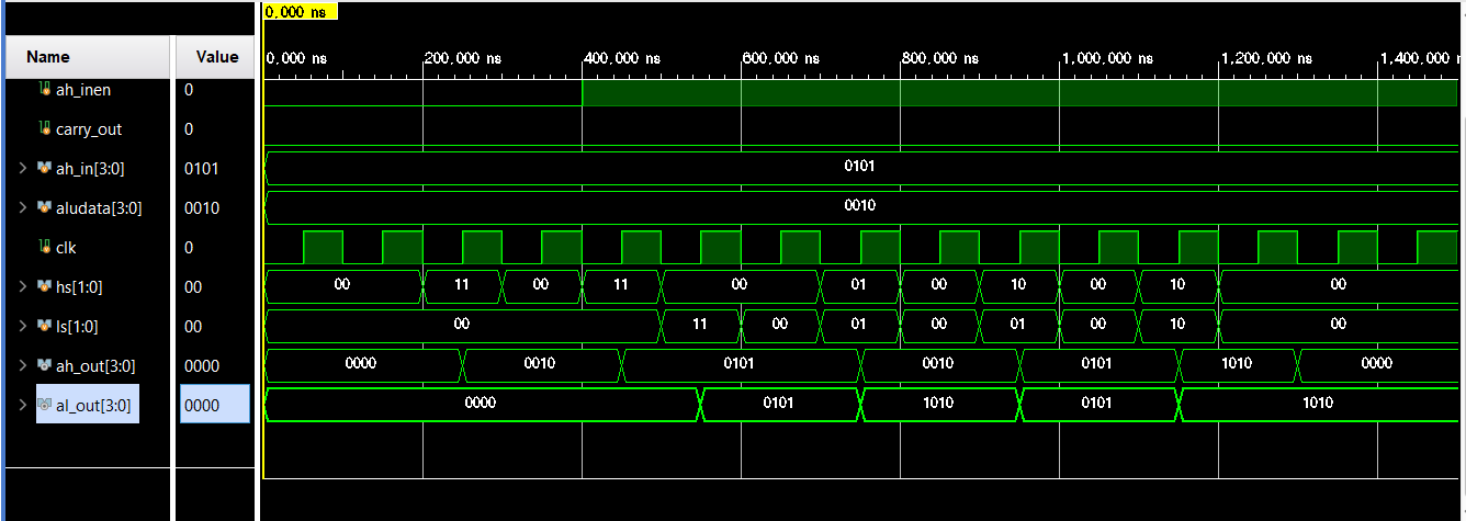
ls가 (1,1)일때를 보면 된다. AH값이 AL로 잘 넘어간 것을 볼 수 있다.
결론
4to1 MUX를 사용하여 universal shift register를 만들었고 2개의 shift register(AH,AL)로 ACC를 만들었다.

참고자료
- IDEC 강의
- universal shift register
https://www.youtube.com/watch?v=4UIIBCVU3gY
'프로젝트 > 4bit CPU' 카테고리의 다른 글
| [4bit CPU #6] control unit(2) (control block) - 18EE (0) | 2023.07.21 |
|---|---|
| [4bit CPU #5] Control unit(1) (Decoder / Ring counter) - 18EE (0) | 2023.07.17 |
| [4bit CPU #4] ALU+ACC (feat.MUL/DIV) - 18EE (0) | 2023.07.16 |
| [4bit CPU #3] ALU - 18EE (0) | 2023.07.15 |
| [4bit CPU #1] Register, Program Counter(PC) - 18EE (0) | 2023.07.12 |
- Total
- Today
- Yesterday
- 굿노트 내보내기
- 굿노트 녹음파일
- DVFS
- acc
- MTCMOS
- mp3파일 추출
- Control Unit
- 4bit CPU
- dynamic power
- VLSI 전력소모
- VLSI power
- 굿노트 mp3파일 추출
- CMOS power
- VLSI dynamic power consumption
- leakage
- switching power
- level shifter
- 4bit
- Verilog
- CPU
- Stack effect
- vlsi
- static power
- VTCMOS
- ALU
- data gating
- clock gating
- power gating
- delay
- 굿노트 mp3 내보내기
| 일 | 월 | 화 | 수 | 목 | 금 | 토 |
|---|---|---|---|---|---|---|
| 1 | 2 | 3 | 4 | 5 | 6 | 7 |
| 8 | 9 | 10 | 11 | 12 | 13 | 14 |
| 15 | 16 | 17 | 18 | 19 | 20 | 21 |
| 22 | 23 | 24 | 25 | 26 | 27 | 28 |
| 29 | 30 | 31 |