
티스토리 뷰
IDEC 강의 영상을 보고 정리한 내용입니다.
https://www.idec.or.kr/vod/apply/view/?pay=&search_val=CPU&no=273
반도체설계교육센터
강의제목 CPU 설계 및 응용 구분 부산대 / 설계강좌 / 초급/중급 / 이론+실습 강의시간 13시간 열람기간 16일 이용료(일반) 무료 이용료(학생) 무료 강의개요 SoC 설계를 위해서 CPU를 설계하고 응용할
www.idec.or.kr
저번까지 설계한 CPU의 구조이다.

저번까지 MUL/DIV연산이 가능하도록 ALU와 ACC의 구성을 마쳤다. 이제 control block을 만들어야한다.
CPU 동작 과정

CPU는 main memory에 있는 명령어를 불러와 해독하고 signal 신호를 만들어 각 module을 동작시킨다.
이때 명령어를 불러오는 과정을 fetch cycle이라고 부르고
명령어를 해독하고 signal 신호를 만들어 module을 동작시키는 과정을 Execution cycle이라고 부른다.
Fetch cycle

fetch cycle은 총 3번의 clock을 소비하여 이뤄진다.
fetch cycle이 끝나면 IR이 업데이트되고 이는 control unit과 연결되어있다.
Execution cycle

강의 자료의 예시이다. MOV TMP,BR은 TMPREG의 내용을 BREG로 옮기라는 명령어이다.
이때 control unit은 tmp_oen, breg_inen을 1로 만들어 temp register의 내용을 breg register에 흘려줘야한다.
위의 내용을 정리하면
t0-t2(3 clock) : fetch cycle
t3(1 clock) : execution cycle
이라고 볼 수 있다.
Decoder, Ring counter
Control unit은 decoder를 이용하여 명령어를 해독하고 ring counter를 이용하여 타이밍에 맞는 signal 신호를 내보낸다.
Decoder
다음은 이번 강의에 사용된 명령어를 정리한 것이다.
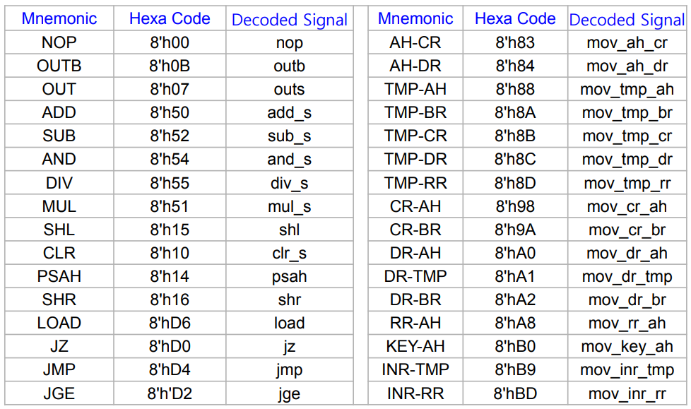
각 명령어를 구분해야한다. Decoder는 case문을 사용하여 구현한다.
`timescale 1ns / 1ps
module decoder(input [7:0] ir_in,
output reg nop,outb,outs,add_s,sub_s,and_s,div_s,mul_s,shl,
clr_s, psah,shr,load,jz,jmp,jge,mov_ah_cr,mov_ah_dr,
mov_tmp_ah, mov_tmp_br,mov_tmp_cr,mov_tmp_dr,
mov_tmp_rr,mov_cr_ah,mov_cr_br,mov_dr_ah, mov_dr_tmp,
mov_dr_br,mov_rr_ah,mov_key_ah,mov_inr_tmp,mov_inr_rr);
always @(ir_in) begin
{nop,outb,outs,add_s,sub_s,and_s,div_s,mul_s,shl,clr_s,
psah,shr,load,jz,jmp,jge,mov_ah_cr,mov_ah_dr,
mov_tmp_ah,mov_tmp_br,mov_tmp_cr,mov_tmp_dr,
mov_tmp_rr,mov_cr_ah, mov_cr_br,mov_dr_ah,
mov_dr_tmp,mov_dr_br,mov_rr_ah,mov_key_ah,
mov_inr_tmp,mov_inr_rr}=0;
case(ir_in)
8'h00: nop=1;
8'h0B: outb=1;
8'h07: outs=1;
8'h50: add_s=1;
8'h52: sub_s=1;
8'h54: and_s=1;
8'h55: div_s=1;
8'h51: mul_s=1;
8'h15: shl=1;
8'h10: clr_s=1;
8'h14: psah=1;
8'h16: shr=1;
8'hD6: load=1;
8'hD0: jz=1;
8'hD4: jmp=1;
8'hD2: jge=1;
8'h83: mov_ah_cr=1;
8'h84: mov_ah_dr=1;
8'h88: mov_tmp_ah=1;
8'h8A: mov_tmp_br=1;
8'h8B: mov_tmp_cr=1;
8'h8C: mov_tmp_dr=1;
8'h8D: mov_tmp_rr=1;
8'h98: mov_cr_ah=1;
8'h9A: mov_cr_br=1;
8'hA0: mov_dr_ah=1;
8'hA1: mov_dr_tmp=1;
8'hA2: mov_dr_br=1;
8'hA8: mov_rr_ah=1;
8'hB0: mov_key_ah=1;
8'hB9: mov_inr_tmp=1;
8'hBD: mov_inr_rr=1;
default : nop=1;
endcase
end
endmodule
`timescale 1ns / 1ps
module tb_decoder;
reg [7:0] ir_in;
wire nop,outb,outs,add_s,sub_s,
and_s,div_s,mul_s,shl, clr_s,
psah,shr,load,jz,jmp,jge,mov_ah_cr,mov_ah_dr, mov_tmp_ah,
mov_tmp_br,mov_tmp_cr,mov_tmp_dr,mov_tmp_rr,mov_cr_ah,
mov_cr_br,mov_dr_ah, mov_dr_tmp,
mov_dr_br,mov_rr_ah,mov_key_ah,mov_inr_tmp,mov_inr_rr;
decoder UUT(ir_in,
nop,outb,outs,add_s,sub_s,and_s,div_s,
mul_s,shl,clr_s, psah,shr,load, jz,jmp,jge,
mov_ah_cr,mov_ah_dr, mov_tmp_ah,
mov_tmp_br, mov_tmp_cr,mov_tmp_dr,
mov_tmp_rr,mov_cr_ah,mov_cr_br,
mov_dr_ah, mov_dr_tmp,
mov_dr_br,mov_rr_ah,
mov_key_ah,mov_inr_tmp,mov_inr_rr);
initial begin
ir_in = 0;
#100; ir_in = 8'h0B;
#100; ir_in = 8'h07;
#100; ir_in = 8'h50;
#100; ir_in = 8'h52;
#100; ir_in = 8'h54;
#100; ir_in = 8'h55;
#100; ir_in = 8'h51;
#100; ir_in = 8'h15;
#100; ir_in = 8'h10;
#100; ir_in = 8'h14;
#100; ir_in = 8'h16;
#100; ir_in = 8'hD6;
#100; ir_in = 8'hD0;
#100; ir_in = 8'hD4;
#100; ir_in = 8'hD2;
#100; ir_in = 8'h83;
#100; ir_in = 8'h84;
#100; ir_in = 8'h88;
#100; ir_in = 8'h8A;
#100; ir_in = 8'h8B;
#100; ir_in = 8'h8C;
#100; ir_in = 8'h8D;
#100; ir_in = 8'h98;
#100; ir_in = 8'h9A;
#100; ir_in = 8'hA0;
#100; ir_in = 8'hA1;
#100; ir_in = 8'hA2;
#100; ir_in = 8'hA8;
#100; ir_in = 8'hB0;
#100; ir_in = 8'hB9;
#100; ir_in = 8'hBD;
#100;
end
endmodule
명령어에 맞는 ouput이 high가 된 것을 볼 수 있다.
Ring counter
한 명령어를 실행할 때 clock에 맞춰 순차적으로 제어신호가 생성되어야한다. 이때 ring counter는 clock 타이밍을 잡아주는 역할을 한다.
한 명령어가 실행되기위해 최대 12번의 clock(MUL,DIV)이 필요하기때문에 t0-t11의 ouput이 필요하다.
더 자세한 내용은 다음 게시물에 올리겠다.
module ringCounter(clk,clr,t);
input clk, clr;
output [11:0] t;
reg [11:0] st=0;
always @(negedge clk, posedge clr) begin
if (clr==1) st=12'b0;
else if (st==12'b0) st=st+1;
else if (st==12'b100000000000) st=12'b000000000001;
else st=st<<1;
end
assign t=st;
endmodule
`timescale 1ns / 1ps
module tb_ringCounter;
reg clk, clr;
wire [11:0] t;
ringCounter UUT(clk,clr,t);
always #50 clk=~clk;
initial begin
clk=0;
clr=0;
end
endmodule
t0-t11output이 순차적으로 high가 되는 것을 볼 수 있다. 이 신호에 맞춰 control신호를 내보내면 된다.
결론
control unit을 만들기위해 decoder와 ring counter를 설계했다.
다음에는 각 명령어에 맞게 실제 control신호를 생성하는 것을 하겠다.
참고자료
- 아이덱 강의
- CPU 동작과정 : https://blog.naver.com/PostView.naver?blogId=ben4109&logNo=222284380523
컴퓨터 구조 - 명령어 실행
명령어 실행에 대해서 자세하게 알아보겠습니다. . . . 명령어의 실행 명령어의 실행은 전 포스트에서 명령...
blog.naver.com
'프로젝트 > 4bit CPU' 카테고리의 다른 글
| [4bit CPU #6] control unit(2) (control block) - 18EE (0) | 2023.07.21 |
|---|---|
| [4bit CPU #4] ALU+ACC (feat.MUL/DIV) - 18EE (0) | 2023.07.16 |
| [4bit CPU #3] ALU - 18EE (0) | 2023.07.15 |
| [4bit CPU #2] ACC(Universal shift register) - 18EE (0) | 2023.07.12 |
| [4bit CPU #1] Register, Program Counter(PC) - 18EE (0) | 2023.07.12 |
- Total
- Today
- Yesterday
- 굿노트 mp3파일 추출
- leakage
- 4bit CPU
- level shifter
- VTCMOS
- VLSI 전력소모
- Control Unit
- ALU
- DVFS
- clock gating
- switching power
- VLSI dynamic power consumption
- delay
- mp3파일 추출
- CMOS power
- power gating
- data gating
- 굿노트 mp3 내보내기
- static power
- 굿노트 녹음파일
- dynamic power
- VLSI power
- acc
- 굿노트 내보내기
- 4bit
- Stack effect
- vlsi
- MTCMOS
- CPU
- Verilog
| 일 | 월 | 화 | 수 | 목 | 금 | 토 |
|---|---|---|---|---|---|---|
| 1 | 2 | 3 | 4 | 5 | 6 | 7 |
| 8 | 9 | 10 | 11 | 12 | 13 | 14 |
| 15 | 16 | 17 | 18 | 19 | 20 | 21 |
| 22 | 23 | 24 | 25 | 26 | 27 | 28 |